Tuesday, October 31, 2023
Free Enterprise and Social Mobility by Dan Mitchell
At the risk of understatement, our friends on the left are fixated on equality.
 If they were talking about equality of opportunity, or equality before the law, that would be great.
Unfortunately, they want equality of outcomes. Which means supporting bigger government, higher taxes, and other policies that are likely to shrink the economic pie.
In a just and sensible society, the goal should instead be upward mobility so that everyone can get richer.
That means enacting policies that expand the economic pie.
And what are those policies? We can answer that question by looking at a new study by Professors Justin Callais, Vincent Geloso, and Alicia Plemmons. Published by the Archbridge Institute, it investigates whether there is a link between limited government and social mobility.
…an increasing share of debates in economics have centered on the study of inequality… Intricately tied to these debates is the topic of social mobility.
…Using the recent data of Chetty et al…on social capital and intergenerational income mobility in the United States at the subnational-level, we…ask…whether a) economic freedom does improve intergenerational mobility in a meaningful way when using higher quality data and; b) whether economic freedom complements or substitutes the different types of social capital.
Here’s what they found.
…we find that a) economic freedom (both in aggregate form and its components) is tied to greater absolute and relative mobility; b) we find that it has no association with the racial gap in mobility; c) we find that the effect of economic freedom generally outweighs that of inequality; d) the effect of economic freedom matches those of “bridging” social capital and overpowers that of other forms of social capital. …Table 2 regresses the four economic freedom measures against absolute, relative, and gap mobility. Note, each cell within the table represents a separate regression of one measure of economic freedom against one measure of economic mobility, which results in twelve separate regressions. …we find that (low levels) of government spending and high values of labor market freedom are highly correlated with increases in both absolute and relative mobility.
Here is the aforementioned Table 2 for data geeks.

Looking at the conclusion of the study, here are some key takeaways.
While the literature is already clear on the fact that economic freedom increases incomes, this study is the first within the United States to show that the effect of economic freedom helps those at the bottom more relative to those at the top. …Policymakers should seriously consider laxer government regulations in the labor market, as well as lowering taxes and government spending as a way to positively impact those who wish to move up the income ladder.
Sounds like a familiar recipe.
MATCHING TO THE COMPLEX LOAD IMPEDANCE OF A SHORTENED, NON-RESONANT ANTENNA – PART II by MARTIN BLUSTINE
Introduction
In Part I of this article[1], a method for matching the complex load impedance of shortened, non-resonant antennas using L-matching networks and resonators was described. First, we matched to the real part of the complex load impedance, ignoring the imaginary part – the reactance part – until the real part had been matched with an L-matching network. Then, we resonated out the imaginary, reactive part to cancel it, at least at a single design frequency. The technique of reactive absorption was also demonstrated to further simplify matching networks.
Some years ago, Phil Salas, AD5X, presented an interesting approach for matching non-resonant antennas in his QST articles[2][3]. In these, he describes a method for feeding a 43′ vertical antenna with a base-loading network. In his matching technique, he reverses the process used in Part I. First, he resonates out the imaginary part of the complex, capacitive load reactance with an antenna base-loading coil. Once that has been accomplished, he steps up the 50 ohm, real source impedance with a 4:1 voltage UNUN to a convenient, higher real impedance, 200 ohms. Finally, he locates a place on the base-loading coil that matches the stepped-up, 200 ohm, real source impedance. Procedures are provided for resonating away the reactance of the antenna load and for locating the position of the tap.
This article recaps the methods used in Part I and presents a new method for simplifying matching networks. Eventually, this leads us to AD5X’s solution for base-matching a 43′ non-resonant vertical antenna.
Discussion
Figure 1 illustrates AD5X’s method. A 4:1 UNUN transforms the 50 ohm transmitter impedance to 200 ohms. This follows because a 4:1UNUN has a turns ratio of 2:1 and the impedance transformation goes as the square of the turns ratio, N2 = 4. This results in a feed-point at a practical location on the base-loading coil and at a reasonable voltage, too, since the UNUN only increases the voltage by a factor of 2. For a 100 Watt transmitter, the voltage would be stepped up from 70.7 VRMS to 141.4 VRMS and for a 1500 Watt transmitter, the voltage would be stepped up from 274 VRMS to 548 VRMS. By practical location, it is meant that the feed-point is located at some distance from the end of the inductor so that adjustments may be made.
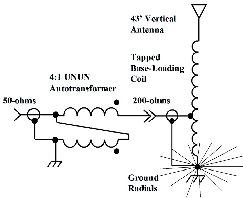
Figure 1. A 4:1 UNUN Feeds A Tapped Base-Loading Coil. The base-loading coil is tuned to resonate out the capacitive reactance of the shortened antenna. A point is found on the base-loading coil to inject the signal from the 4:1 UNUN and to achieve a match. Please click on the figure to enlarge.
Since the voltage increases by a factor of 2, the current must decrease by a factor of 2 according to physical law. The entire base-loading coil is tuned to be resonant with the antenna load capacitance (for our case 204.3pf) at the design frequency. This is the same technique that was used in Part I[4].
There is another way to think about the base-loading coil, however. It may be drawn as an L-network. The base-loading coil may be drawn as a parallel element and a series element, Figure 2. Instead of a conventional LC L-network, a less commonly used LL L-network is shown. This will be discussed in detail towards the end of this paper.
If operation on more than one band is desired, the base-loading inductor must be tuned to a new value to resonate with the antenna’s capacitive reactance in the new band. The tap position must also be moved. These changes may be implemented with movable jumpers[5], or they may be automated with relays[6].
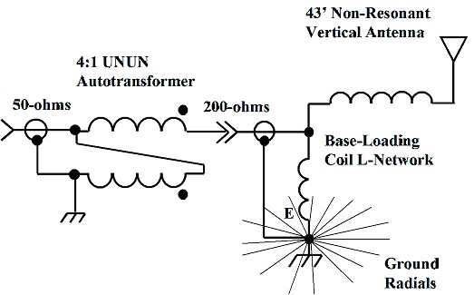
Figure 2. A Simple LL Network. This LL network consists of two windings in series. It is easier to think about this device as a special case of an L-matching network. For multi-band operation, the inductor has to be re-resonated and the tap must be moved. This may be implemented with jumpers, or with relays. Please click on the figure to enlarge.
Commonly and Less Commonly Used L-Network Topologies
Part I described the four most common topologies for L-matching networks, shown in Figure 3[7]. These are not the only ones. There are four other simple L-networks, shown in Figure 4, that prove useful under some conditions, particularly if suitable inductors or capacitors are unavailable. For more information about these topologies, please refer to a book on the subject of Smith Charts such as Phillip Smith’s, Electronic Applications of the Smith Chart[8].
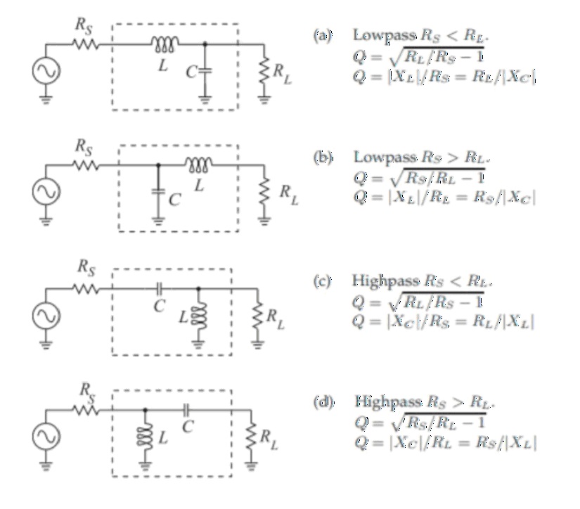 Figure 3. Four Commonly Used L-Matching Network Topologies. These topologies may be used to map and match the entire complex impedance plane. Please click on the figure to enlarge. Reproduced under CC BY-NC by permission of Michael Steer, North Carolina State University.
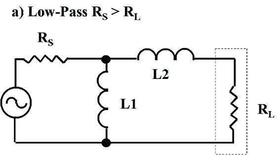
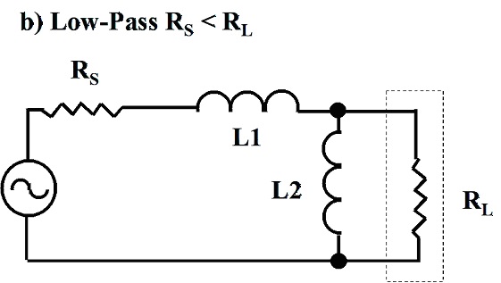
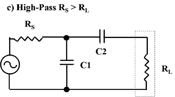
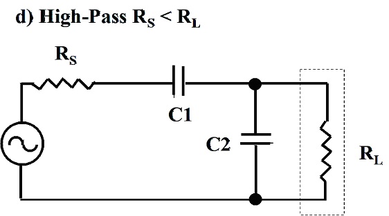
Figure 4. Four Less Commonly Used L-Matching Network Topologies. At a) and b), low-pass topologies. At c) and d), high-pass topologies. These topologies may be useful if suitable inductors or capacitors are unavailable. These topologies may be used to map limited portions of the complex impedance plane. The low-pass LL-version, RS > RL, is exploited towards the end of this paper. Please click on the figure to enlarge.
Modeling of a 43′ Non-Resonant Vertical Antenna in EZNEC
A 43′ non-resonant vertical antenna was modeled at 3.6 MHz in EZNEC[9] to find the unmatched feed-point impedance. For this case, 60 radial wires, 66′ (20.1m) in length (~1/4l) were used. The radials were placed 0.01m above the ground so that EZNEC could be used to model them. EZNEC instructions state that for wires placed low to the ground, the Real/High Accuracy ground type must be selected[10]. The soil conductivity was set to 6 mS/m, while the dielectric constant was set to 13.
The 43′ antenna model is shown in Figure 5. This model utilizes wire for the 43′ vertical. It could just as easily have been replaced with a piece of aluminum tubing. This would alter the antenna impedance. However, for this instructive exercise, it doesn’t matter.
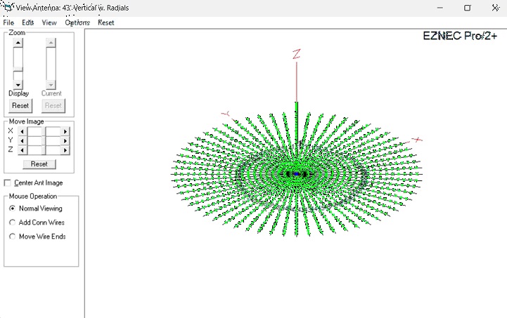 Figure 5. The 43′ Non-resonant Vertical. The radials were modeled at ~1/4λ for 80m. Please click on the figure to enlarge.
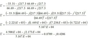
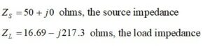
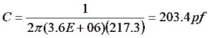
EZNEC was run for a few points to obtain the unmatched impedance at 3.6 MHz. The result is shown in Figure 6. The impedance at the base of the vertical is ZL = 16.69 – j217.3 ohms. The VSWR is shown to be 59.9:1, and this will be calculated directly from the unmatched impedance. The capacitive reactance, -j217.3 ohms, equates to 203.4 pf at 3.6 MHz.
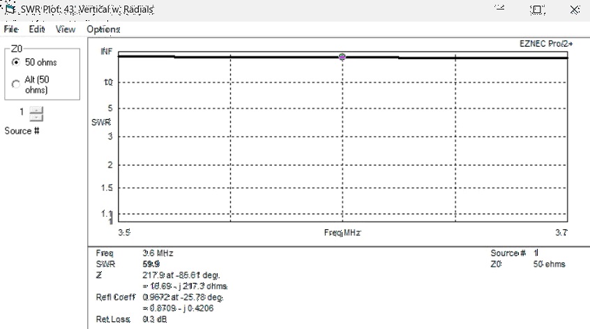
Figure 6. EZNEC Plot of the Unmatched 43′ Antenna with Radials. The frequency span is 3.5 to 3.7 MHz. The VSWR is calculated in a 50 ohm system. Please click on the figure to enlarge.
Calculation of the Unmatched VSWR from the Load Impedance
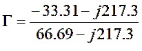
The unmatched VSWR is calculated from the simulated antenna load impedance ZL = 16.69 – j217.3 ohms. To determine the VSWR, the input voltage reflection coefficient is calculated for the unmatched antenna. The input voltage reflection coefficient is a measure of how much of the voltage wave incident at the unmatched antenna discontinuity is reflected back toward the RF source. As the voltage reflection coefficient approaches unity, more of the incident wave is reflected from the antenna discontinuity back toward the transmitter or signal source. The voltage reflection coefficient is calculated from
where
ZL is the complex load impedance of the antenna as simulated in EZNEC, or measured with a vector antenna analyzer, in units of ohms.
ZS is the complex impedance of the signal source, which could be the transmitter, or a vector antenna analyzer, in units of ohms.
For the time being, we ignore the 4:1 UNUN and provide a match between a 50 ohm source and the complex load impedance. The 200 ohm source impedance is introduced into the simulation for Example 3.
Given,
![]()
![]()
the value of the complex reflection coefficient is given by
![]()
Combining terms, where possible
Method I – Rectangular Form
Rationalize the denominator
The magnitude of the reflection coefficient is given by
![]()
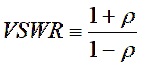
The voltage standing wave ratio is defined by

The VSWR of the unmatched 43′ vertical is 59.97:1. This agrees with the EZNEC result.
Method II – Polar Form
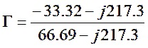
and let
![]()
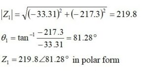
and let
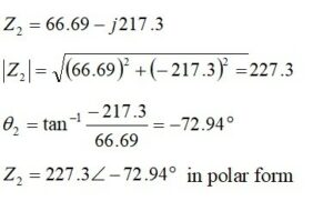
Dividing, we obtain
![]()
Moving the angle from the denominator to the numerator changes the sign.
![]()
All we need is the magnitude, and it agrees with Method I
![]()
VSWR is defined by
![]()
For exercise , we may convert from polar form back to rectangular form
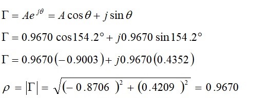
This value of the magnitude of the reflection coefficient agrees with the first result for a VSWR of 59.61:1.
Return Loss
The return loss is a measure of the loss of signal power due to mismatch between the source impedance and the unmatched load impedance. By IEEE convention, the return loss is always expressed as a positive number in units of dB. The lower the return loss, the worse the mismatch is.
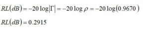
This agrees with the EZNEC result.
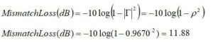
Mismatch Loss
If the antenna load impedance is mismatched to the source, the loss in units of dB will be
Forward Power
The forward power, expressed in units of percent, is
![]()
Reflected Power
The reflected power, expressed in units of percent, is

Impedance Matching Techniques Using L-Networks – 50 ohm Source Impedance
In Part I, techniques for matching with L-networks were introduced. In this section, L-networks will be used to match a 50 ohm source to the mismatched 43′ antenna. (We will visit the case of the 200 ohm source later.) Once the real part of the complex antenna load impedance has been matched, the reactive part will be canceled using the reactance adsorption technique for the first two examples. A new technique will be used for the third example.
It is known from Figure 3 that the equations in the following sections apply for RS > RL.
Example 1 – Low-Pass Topology with Reactance Adsorption
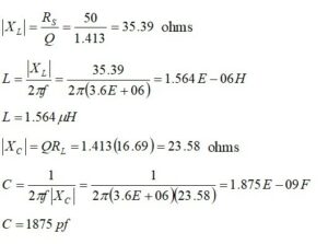
We write down the equations that will match a real source impedance of 50 ohms to a real load impedance of 16.69 ohms. Thus, we set the reactive part of the load impedance to zero.
![]()
From Figure 3(b), we learn that for
![]()
the unloaded Q is calculated from
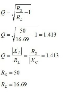
The L-network reactances and component values are calculated from

We are not done yet because we have ignored the reactive part of the antenna load impedance. This is, after setting the real part to zero
![]()
This impedance is equivalent to a capacitance of

We remember that to cancel a negative reactance, we need an equal but opposite positive reactance. So, we need a positive inductive reactance of
![]()
to cancel the negative capacitive reactance of the load impedance.
The required inductive reactance is calculated from

This resonating inductance may be combined with the series inductance in the matching network for a total inductance of
![]()
This matching network may be modeled in RFSim99 with the following results. Figure 7 shows the circuit model, while Figure 8 reports a return loss of 55 dB. Figure 7 does not combine the series inductors. They could be combined, but they have been modeled separately for clarity. The simulation result is the same.
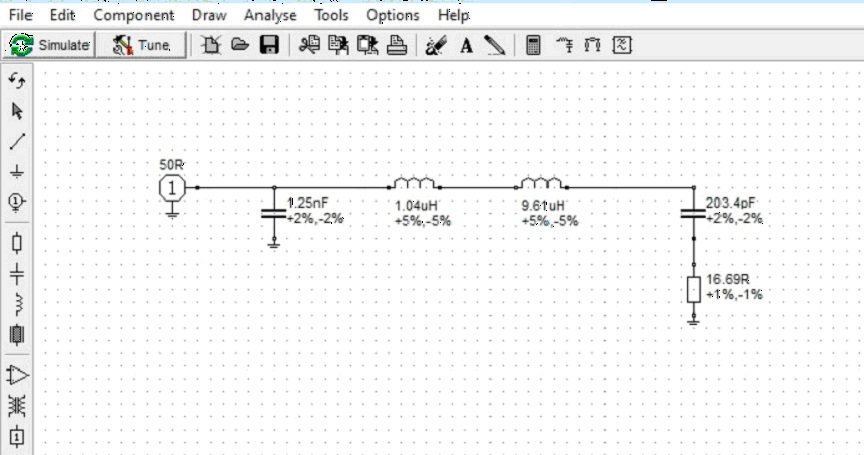
Figure 7. Circuit Model of Low-Pass Topology. The low-pass network matches the 50 ohm source impedance to the antenna complex load. The resonating inductor has not been combined with the L-network inductor for clarity. See text. Please click on the figure to enlarge.
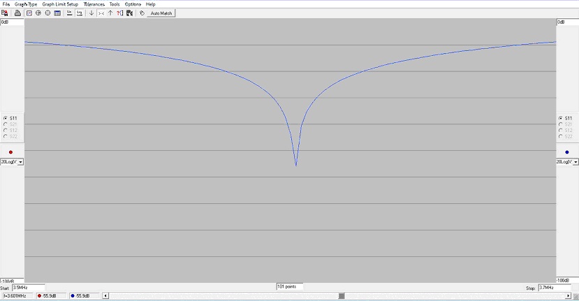
Figure 8. Plot of the Low-Pass Topology Return Loss. This simulation is for the 50 ohm source impedance to antenna complex load match. The return loss is better than 55 dB at 3.6 MHz. Please click on the figure to enlarge.
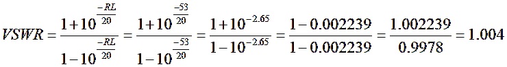
Calculate the VSWR
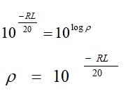
Let’s calculate the VSWR from the return loss. The return loss is defined as
![]()
If we solve for the magnitude of the reflection coefficient, we have
![]()
Finding the antilog of both sides, we obtain
VSWR is defined as
Substituting, we obtain
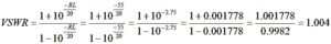
The VSWR is 1.004:1.
From the graph, the 2:1 VSWR bandwidth for this low-pass L-network is 180 kHz. This is based on a return loss of 9.54 dB for a 2:1 VSWR.
Now that the low-pass solution has been modeled, let’s perform a similar analysis for the high-pass solution.
Example 2 – High-Pass Topology without Reactance Adsorption

We write down the equations that will match a real source impedance of 50 ohms to a real load impedance of 16.69 ohms. Thus, we set the reactive part of the load impedance to zero.
![]()
From Figure 3(d), we learn that for
![]()
the unloaded Q is calculated from

The L-network reactances and component values are calculated from
As before, we are not finished because we have ignored the reactive part of the antenna load impedance. This is
![]()
after setting the real part of the load impedance to zero.
This impedance is equivalent to a capacitance of
![]()
We remember that to cancel a negative reactance, we need an equal but opposite positive reactance. So, we need a positive inductive reactance of
![]()
to cancel the negative capacitive reactance of the load impedance.
The required inductive reactance is calculated from
For the high-pass configuration of Figure 9, the resonating inductance may not be easily combined with the shunt inductor in the L-network. Later, we will show how the network may be simplified. Meanwhile, let’s model the topology that we have. The simulation results in the return loss plotted in Figure 10. The result is 53 dB at 3.6 MHz.
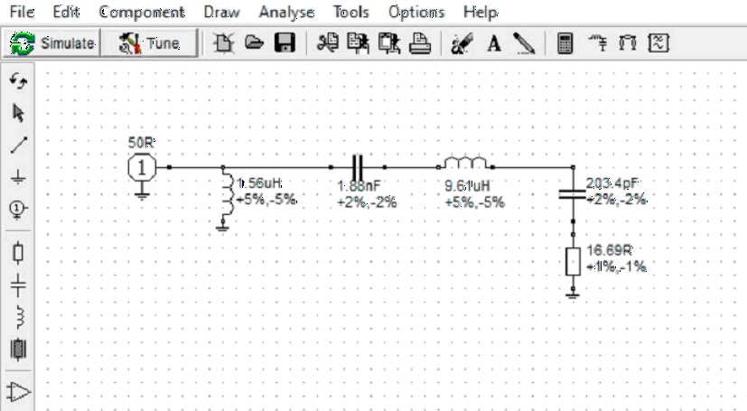
Figure 9. High-Pass L-Network Topology Return Loss. This topology matches a 50 ohm source impedance to the complex antenna load impedance. The resonating inductor is not easily combined with any other component in the L-network. See text. Please click on the figure to enlarge.
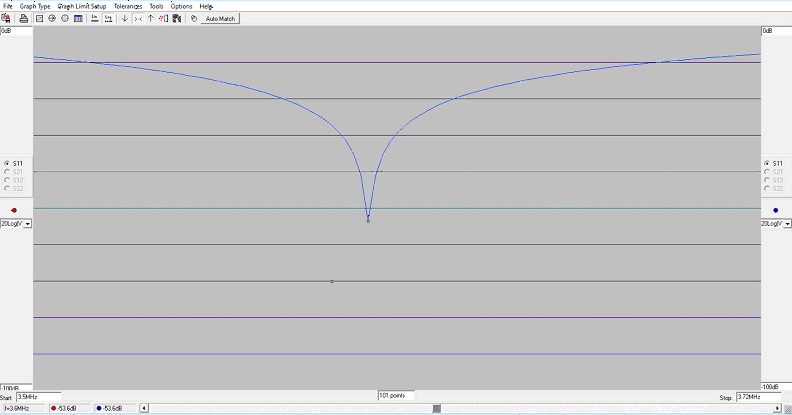
Figure 10. Plot of the High-Pass Topology. This simulation is for the 50 ohm source impedance to antenna complex load match. The return loss is better than 53 dB at 3.6 MHz. Please click on the figure to enlarge.
VSWR Calculation
Substituting, we have
The VSWR is 1.004:1.
The 2:1 VSWR bandwidth for this high-pass L-network is also 180 kHz. This is based on a return loss of 9.54 dB for a 2:1 VSWR. This bandwidth is consistent with the value reported for the low-pass L-network.
Example 3 – High-Pass to Low-Pass Transformation by Partial Reactance Absorption
This is an interesting solution to our impedance matching problem. It puts a number of the tools that we have learned to work and provides an interesting path for simplifying the results from Example 2.
Since our matching network begins with a 4:1 UNUN, that transforms 50 ohms to 200 ohms, and we can change the source impedance for our calculations from 50 ohms to 200 ohms.
We begin, as before, by writing down what we know.
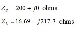
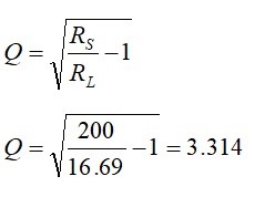
We write down the equations that will match a real source impedance of 200 ohms to a real load impedance of 16.69 ohms. Thus, we set the reactive part of the load impedance to zero.
![]()
From Figure 3(d), we learn that for
![]()
the unloaded Q is calculated from
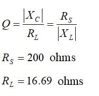
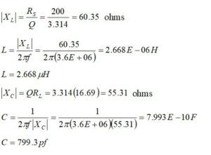
The L-network reactances and component values are calculated from
As before, we are not done yet because we have ignored the reactive part of the antenna load impedance. This is
![]()
after setting the real part of the load impedance to zero.
This impedance is equivalent to a capacitance of

We remember that to cancel a negative reactance, we need an equal but opposite positive reactance. So, we need a positive inductive reactance of
![]()
to cancel the negative capacitive reactance of the load impedance.
The required inductive reactance is calculated from
The circuit model for our matching network is shown in Figure 11. Note that, as was the case for Example 2, the resonating inductor is not readily combined with the other inductor in the matching network. We will fix this. The return loss, Figure 12, is better than 64 dB at 3.6 MHz.
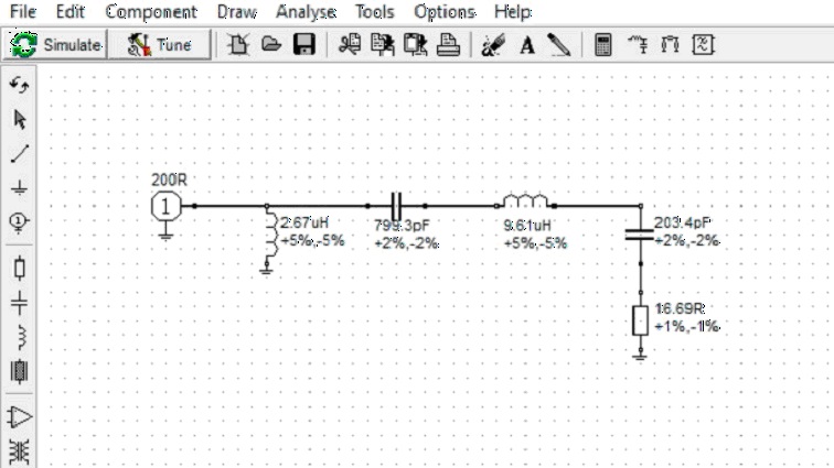
Figure 11. High-Pass L-Network with Resonating Inductance Return Loss. The resonating inductance is not easily combined with the shunt inductor at the input. This will be remedied in the next step. Please click on the figure to enlarge
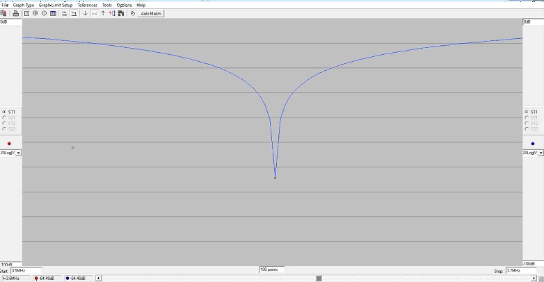
Figure 12. High-Pass L-Network Return Loss. The return loss at 3.6 MHz is better than 64 dB. Please click on the figure to enlarge.
The circuit model for the high-pass topology includes a resonating inductor that cannot be easily absorbed. Is there any transformation that can be applied to simplify the circuit? It turns out that there is. The key to this transformation is to write the series elements in the matching network in terms of their algebraic reactances in ohms.
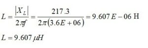
Please recall that the 799.3pf capacitor had a complex reactance of -j55.31 ohms. The 9.607μH inductor had a complex reactance of +j217.3 ohms. If we add the two together, we obtain
![]()
The plus sign indicates that, at least at 3.6 MHz, we could replace the 799.3pf capacitor and the 9.607μH inductor with a single inductor possessing a reactance of +j162.0 ohms.
It is easy enough to work out the inductance value from

This is an interesting result. We have replaced an LC high-pass network with a resonating inductance with an LL low-pass network consisting of a shunt inductor at the input followed by a series inductor.
Now, it is time to go back to the model and see what happens. You might want to find the 2:1 bandwidth and calculate the VSWR from the return loss of this topology. Hint: The 2:1 bandwidth may be read off the plot between the -9.54 dB points. Hint: Use the formula for converting return loss to VSWR that appears in Example1 and Example 2.
Figure 13 shows the circuit model for the partially absorbed resonant inductive reactance. This topology employs one of the lesser-used LL L-matching networks. Networks of this type will match reduced portions of the complex plane, but the transformation topology works for us in this example.
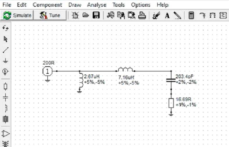
Figure 13. Low-Pass LL Circuit Model with Partial Reactance Adsorption of the Resonating Inductor. This topology is one of the less-used L-matching networks. Networks of this type will match reduced portions of the complex plane, but the transformation topology works for us in this example. Please click on the figure to enlarge.
Figure 14 plots the simulation results for the low-pass LL L-network that is the result of transforming the high-pass network LC L-network. The ~200 kHz bandwidth appears to be somewhat of an improvement over the other topologies. The return loss is better than 59 dB.
We calculate the VSWR as we have done before

The VSWR is 1.0022:1. As an exercise, try calculating the mismatch loss, forward power and reflected power following steps outlined earlier to see the improvement.
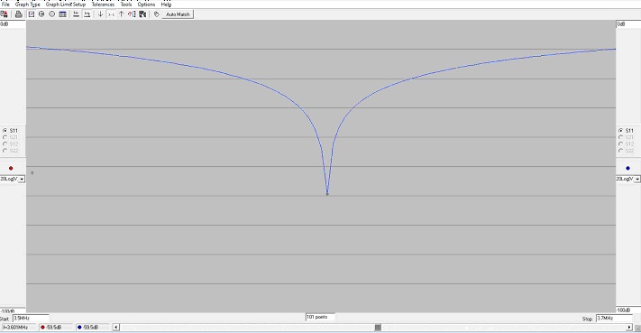
Figure 14. Return Loss of the Low-Pass LL L-Network. The ~200 kHz bandwidth appears to be somewhat of an improvement over the other topologies. See text. The return loss is better than 59 dB for a VSWR of 1.0022:1. Please click on the figure to enlarge.
Please note that when entering the values into the RFSim99 circuit models, the values are rounded off by the app. These truncations result in precision errors that degrade the values for return loss. Inevitably, they lead to errors in reading off the 2:1 bandwidths. Nonetheless, the return loss values are excellent for all three of the matched cases.
There may be some cases for non-resonant antennas where an LL L-network will not work. We were fortunate that we could completely absorb the capacitive reactance of the original high-pass L-network. If the capacitive reactance is too large and the resonating inductive reactance is too small, we will be left with a capacitor in our matching network. This simply means that our load impedance is on a part of the complex plane onto which an LL L-network will not map. To learn more about this, please consider giving Phillip Smith’s book[11] a read. He presents a lot of good material on the subject of LL and CC low and high-pass networks including where they map.
Conclusions
This paper has provided a recap of material provided in Part I for a 43′ non-resonant vertical antenna. The method of partial reactive absorption has been introduced. For our mismatched antenna, we were able to convert from an LC high-pass matching solution to an LL low-pass matching solution. This results in a solution that does not require capacitors. This may not always be the case. It depends on where on the complex plane the antenna complex impedance is located. CC solutions are also possible, but not for our value of complex load impedance. As an exercise, try to figure out why. Hint: Smith Chart L-matching network mappings. The matching topologies introduced in Parts I and II are by no means comprehensive. More complex matching networks offer wider bandwidth, and these provide opportunities for future articles. Part III will discuss the topic of high voltages encountered in matching networks as well as high voltages resulting from highly reactive mismatches in non-resonant antennas.
References
[1] Blustine, Martin, K1FQL, Matching to the Complex Load Impedance of a Shortened, Non-Resonant Antenna – Part I, N1FD Article, July 6, 2023. https://www.n1fd.org/2023/07/06/matching-antenna-part-i/
[2] Salas, Phil, AD5X, 160 and 80 Meter Matching Network for Your 43 Foot Vertical – Part 1, QST, Dec. 2009, pp. 30 – 32.
[3] Salas, Phil, AD5X, 160 and 80 Meter Matching Network for Your 43 Foot Vertical – Part 1, QST, Jan. 2010. pp. 1 – 4. https://www.arrl.org/files/file/QST%2520Binaries/QS0110Salas.pdf
[4] Blustine, July 6, 2023, op. cit.
[5] Salas, Dec. 2009, op. cit.
[6] Salas, Jan. 2010, op. cit.
[7] Blustine, July 6, 2023, op. cit.
[8] Smith, Philip H., Electronic Applications of the Smith Chart, p. 115, McGraw-Hill 1969. https://www.scribd.com/doc/96997209/78897620-Electronic-Applications-of-the-Smith-Chart-SMITH-P-1969
[9] Lewallen, Roy, EZNEC, Antenna Software by W7EL. https://www.eznec.com/
[10] Lewallen, Roy, EZNEC Pro+ v. 7.0 Printable Manual. https://www.eznec.com/ez70manual.html
[11] Smith, Philip H., op.cit.