Last time, I’ve explained everything you could want to know if you wanted to put an M.2 socket onto your board. Today, let’s build M.2 cards! There’s a myriad of M.2 sockets out there that are just asking for a special card to be inserted into it, and perhaps, it’s going to be your creation that fits.
WHY BUILD CARDS?
Laptops and other x86 mainboards often come with M.2 slots. Do you have a free B-key slot? You can put a RP2040 and bunch of sensors on a B-key PCB as an experimental platform carried safely inside your laptop. Would you like to do some more advanced FPGA experiments? Here’s a miniscule FPGA board that fits inside your laptop and lets you play with PCIe on this same laptop – the entire setup having a super low footprint. Are you looking for an extra PCIe link because you’re reusing your laptop as a home server? Again, your WiFi slot will provide you with that. Want to get some PCIe out of a SteamDeck? Building a M-key 2230 card seems to be your only hope!
 There’s also plenty of space for simpler, less active devices. Do you only have a spare M-key slot, perhaps, an A or E key slot? You can replace your WiFi adapter with an extra SSD for extra storage, or perhaps, the other way around, put a second WiFi card into your second SSD slot for all your wardriving needs! Have you just found some unused SATA port traces on your mainboard? You can do what I did and create a dual-port M.2 card that splits one more SSD socket away from your power rail, that you can wire that extra SATA port to and put a SATA M.2 SSD in. Did you just find out that your chipset can give you entire four SATA ports on the M-key SSD slot? You can do what my friend did, and build a card that breaks these SATA ports out!
Even outside x86, quite a few ARM SBCs will have the same problems – they have a M.2 socket with a specific key, say, B, that doesn’t fit some M.2 extender you just bought – well, turns out you can just make an adapter on your own. What about going beyond the standard? Of course, there’s the SparkFun MicroMod ecosystem I mentioned before. Would you like to develop a MicroMod CPU board that works with a myriad of other devices, or perhaps your own MicroMod sensor? That’s an M.2 card right there; and if you need to create your own ecosystem using M.2, nobody stops you either.
Of course, you could design cards with wholly different kinds of value added. For instance, you could be extracting cash out of audiophiles by designing overpriced ‘audio-grade’ SSDs with fancy electrolytic capacitors on them – wouldn’t want to let all that gold plating to go underappreciated, would you? And, if you’re an SBC maker using an M.2 socket for your expansion slot, when buyers say they want to use your SBC as a router, nobody can stop you from designing an absolutely wacky and gigantic card with four Ethernet sockets on it.
OUTLINING THE CARD
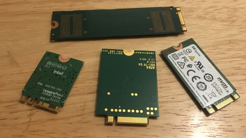
M.2 cards are of standardized sizes – 3042 for 30mm wide 42mm tall, 2260 for 22mm wide 60mm tall; handy thing is, these will be your PCB’s exact dimensions. The screw notch is centered as opposed to mPCIe cards, and is usually a single M.2 screw. You’ll see people saying that the screw is responsible for having a ground connection – it isn’t, even if it might look like it, the ground pins on the receptacle itself are enough, though extra ground paths tend to be nice. In fact, there’s no requirement to have the notch area expose copper, either, it can just be a PCB cutout.
If designing a card for an existing device, it will either be 42 mm or 80 mm long. 30 mm is rare outside the SteamDeck and other low-footprint devices, and 60 mm is super obscure. 22 mm is width for everything except for WWAN slots, those are usually designed with 30 mm card width in mind. Placing all components on a single side of the card isn’t required, though, of course, it will make assembly easier for you. Keep in mind, though, some devices use flat or mid-mount socket, and tall components on the bottom might become a problem you wouldn’t have expected.
M.2 requires a 0.8 mm PCB. You don’t need to have it ENIG, but I recommend it. My understanding is that solder coating done with HASL would oxidise quicker and make worse contact with card sockets – that said, I never tried going with HASL. I am certain that HASL would work well enough for short-term-use prototypes, though! You might think that gold finger treatment is a must, whether with thicker gold on pads or beveled edge of the card – in my experience, neither are required, but thicker gold will increase plug-unplug cycles and a beveled edge will make the card a bit easier to insert. I’ve personally always went with non-beveled regular ENIG and had a great experience.
Of course, you’ll want a card edge footprint in KiCad. I’ve personally been using a KiCad M.2 card edge footprint generator plugin, initially created by @STOP-Pi on GitHub and refactored by me. However, the author deleted their GitHub account at some point, and the plugin no longer loads on KiCad6 – all the generated footprints were done in KiCad5. What’s worse is, between me making my changes and the deletion moment, they even updated the plugin code – and it might’ve been that I missed their KiCad 6 compatibility commits before deletion. Welp, pull requests most welcome! In the meantime, here are the pre-generated A, B, E, M, A+E and B+M card edges that you can already use, and [timonsku] has also made an Eagle library that you should be able to easily convert to KiCad.
INSIDE THE OUTLINE
You might be wondering whether you’d need a four-layer PCB, especially if you want to do PCIe – with four layers, 90 ohm impedance matching is actually achievable, while 0.8 mm distance to ground on two-layer makes it unrealistic. Here’s my experience – I’ve been doing small PCIe adapters for a while now, and they’ve worked quite well on 2-layer, which is a requirement for my specific prototyping workflow. Typically, M.2 cards account for a very short distance proportionally to the length of the entire PCIe link you’ll have, and deviations likely won’t prevent the PCIe link from working – it’s longer distances that might have you experience problems until you upgrade your cabling. I wouldn’t be surprised to see a higher error rate or the link being downgraded to a lower generation during training, but my bets are that your PCIe will function.
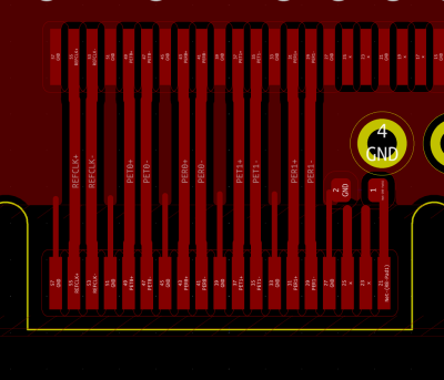 Need to stick with two layers? Do as much impedance matching as you can manage, treat your differential pairs with respect, and your prototypes will work fine – after all, it has been said that PCIe works over wet string, and we’ve witnessed confirmations one after another. My diffpairs are typically 0.35 mm / 0.15 mm, which is within cheap 2-layer process boundaries and results in around 130 ohm impedance, which is imperfect but better than nothing. For stuff like PCIe and SATA, M.2 typically keeps all high-speed diffpairs on the card’s top side, and this alone helps a bunch with aspects like an uninterrupted ground layer under your pairs. If your workflow and budget allows for four layers, go for it!
Add a ground fill plane keepout plane on the area where gold fingers go – otherwise, you might short out a bunch of important host-side pins when inserting the card. The standard also suggests a keepout plane on internal layers under the fingers, so keep that in mind if you go four-layer or beyond.
When stenciling, make sure that solder paste doesn’t get on the M.2 card fingers – clean them well before reflow if it does, because it’s way more painful to get them solder-free after. 0.8 mm PCBs are thin, and if you decide to hot air them, fasten them in a way that doesn’t stress them – I’ve had a few self-designed M.2 cards bend when held in a vise and blasted with a hot air gun that, perhaps, was a bit outside its calibration.
In terms of power, you only get 3.3 V, at an amp or two. This is both a blessing and a curse – it’s plenty of power, and you don’t typically need extra regulation since majority of chips are okay with 3.3 V, but there’s still some good uses for 5 V. Manufacturers that need to get 5 V on a M.2 card, tend to resort to cursed solutions – here’s the story of a Dell adapter creating a 2.5″ HDD socket out of M.2, that redefines one of the GND pins as a proprietary card detection pin and sends 5 V to a group of otherwise reserved pins if that pin is not GND-connected.
RESEARCH AND PROCEED
Designing a card for an existing device and expecting a certain interface? Make sure it’s actually there – as I mentioned, you can expect PCIe on A, E and M sockets, and USB 2.0 on A, E and B sockets, anything else is not a given. if Internet doesn’t help you here, looking for traces coming from the socket could work, but is not always foolproof because signals might be going through vias under the socket. That said, if you can spot traces or diffpair series capacitors, that will be a good indication – or perhaps, using a multimeter for an IC internal diode test on USB2 or single-ended signals like PERST / PEWAKE / CLKREQ would be in order. After all, quite a few laptops have B-key slots that only have USB 3.0 (ThinkPad T460s), or even only USB 2.0 (ThinkPad T470S), despite SATA and PCIe typically being available.
This concludes the “M.2 For Hackers” series. Some things about M.2 might look alien when you see it for the first time, but I hope I could clarify what’s going on, and how you can get in on the action. The M.2 ecosystem is not going away anytime soon, and it helps if we know just how to bend it to our will wherever needed!
No comments:
Post a Comment