This is a simple and experimental modification that transforms a QCX into a (Class-E driven) SSB transceiver. It can be used to make QRP SSB contacts, or (in combination with a PC) used for the digital modes such as FT8. It can be fully-continuous tuned through bands 160m-10m in the LSB/USB-modes with a 2200Hz bandwidth has up to 5W PEP SSB output and features a software-based full Break-In VOX for fast RX/TX switching in voice and digital operations.
The SSB transmit-stage is implemented completely in a digital and software-based manner: at the heart the ATMEGA328 is sampling the input-audio and reconstructing a SSB-signal by controlling the SI5351 PLL phase (through tiny frequency changes over 800kbit/s I2C) and controlling the PA Power (through PWM on the key-shaping circuit). In this way a highly power-efficient class-E driven SSB-signal can be realized; a PWM driven class-E design keeps the SSB transceiver simple, tiny, cool, power-efficient and low-cost (ie. no need for power-inefficient and complex linear amplifier with bulky heat-sink as often is seen in SSB transceivers).
An Open Source Arduino sketch is used as the basis for the firmware, the hardware modification bypasses the QCX CW filter and adds a microphone input in-place of the DVM-circuit; the mod is easy to apply and consist of four wire and four component changes and after applying the transceiver remains compatible with the original QCX (CW) firmware.
This experiment is created to try out what can be done with minimal hardware; a simple ATMEGA processor, a QCX and a software-based SSB processing approach. It would be nice to add more features to the sketch, and try out if the QCX design can be further simplified e.g. by implementing parts of the receiver stage in software. Feel free to experiment with this sketch, let me know your thoughts or contribute here: https://github.com/threeme3/QCX-SSB
73, Guido pe1nnz@amsat.org

List of features:
- EER-alike Class-E driven SSB transmit-stage
- Approximately 5W PEP SSB output (depending on supply voltage, PA voltage regulated through PWM with 36dB dynamic range)
- supports USB and LSB modes up to 2200 Hz bandwidth (receiver and transmitter)
- Receiver unwanted side-band rejection up to 20dB
- Continuously tunable through bands 160m-10m (anything between 20kHz-99MHz)
- Multiband support 3 with the possibility to add I2C filter bank switching in Arduino sketch
- Software-based VOX that can be used as fast Full Break-In (QSK operation) or assist in RX/TX switching for operating digital modes (no CAT or PTT interface required)
- Mod simple to apply (4 wires, 4 components changes and a firmware change)
- Mod remains downwards-compatible with the original firmware (except for the loss of DVM function)
- Firmware is Open Source through an Arduino Sketch, it allows experimentation, new features can be easily added, contributions can be shared via Github repository QCX-SSB.
- Completely digital and software-based SSB transmit-stage (no additional circuitry needed, except for the audio-in circuit)
- ATMEGA328 signal processing: samples audio-input and reconstruct a SSB-signal by controlling the phase of the SI5351 PLL (through tiny frequency changes over 800kbits/s I2C) and the amplitude of the PA (through PWM of the PA key-shaping circuit).
- Lean and low-cost SSB transceiver design: because of the EER class-E stage it is highly power-efficient (no bulky heatsinks required), and has a simple design (no complex balanced linear power amplifier required)
Revision History:
| Rev. | Author | Description |
|---|---|---|
| R1.00 | pe1nnz@amsat.org | Initial release of prototype |
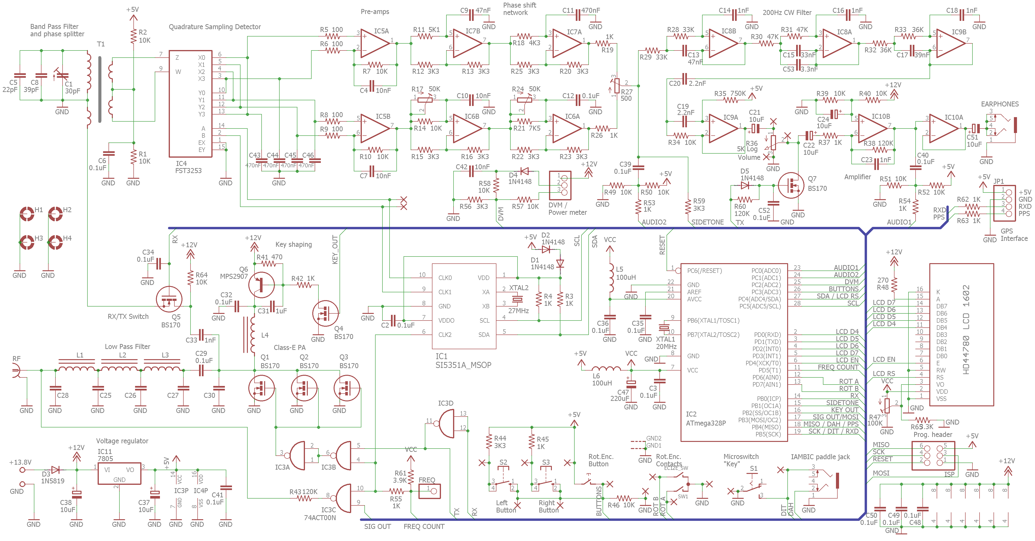
Schematic:
RX mod (step 1):
            (CW filter)         CW
    ──┐     to IC9A/pin1 ────────o    SW    C21[]│
     ┌┴┐                             o─────────[]│────to LF amp
     │ │  (I/Q phase net)           /         +[]│
     │ │<────────────────────────o /
     └┬┘  to R27/pin2          SSB      RX 3dB BW
    ──┘                               (200/2200Hz)
Audio-input mod (step 2-5, changes the DVM circuit):
                          5V┌─────────┐
               ┌────────────┤AVCC 20  │
               │        1.1V│         │
             D4│     R57┌───┤AREF     │
            10K│     10K│   │21       │
              ┌┴┐      ┌┴┐  │         │
              │ │      │ │  │ATMEGA328│           (Step 7 - only for ISP programming)
              │ │      │ │  │   QCX   │           ┌─────────┐
              └┬┘      └┬┘  │         │ISP-2      │ Arduino │
   Paddle/Tip  │   ||   │   │    RESET├───────────┤10       ├────[USB+cable to PC with Arduino
    ┌──────────+───||───+───┤ADC2     │ISP-3      │    UNO  │
    │Electret  │R58||   │   │25   MOSI├───────────┤11       │
    │mic       │ 220nF ┌┴┐  │         │ISP-6      │         │
   |O        ──┴──     │ │  │     MISO├───────────┤12       │
    │        ──┬──     │ │  │         │ISP-4      │         │
    │      C42 │    R56└┬┘  │      SCK├───────────┤13       │  <-- runs ArduinoISP
    │      10nF│    10K │   │22       │ISP-1      │         │
    └──────────┴────────┴───┤GND   GND├───────────┤GND      │
   Paddle-jack/Sleeve       └─────────┘           └─────────┘
Original QCX Schematic: 
Installation:
You will need to install 4 wires, change 4 components and upload the firmware of this sketch:
- Disconnect +/side of C21 from IC9/pin1 and wire +/side of C21 to R27/pin2, you may1 insert SPDT switch with common to C21 and the throws to IC9/pin1 and R27/pin2 for SSB/CW switching
- Remove D4, insert resistor 10K in D4
- Move R58 (10K) to R56, insert capacitor 220nF in R58
- Move C42 (10nF) to the backside of PCB and place it on the top pads of D4 and C42 that are closest to IC2
- Wire DVM/pin3-R57 to IC2/pin21 (AREF), wire junction D4-C42-R58 to IC2/pin18 (DAH), wire DVM/pin2 to IC2/pin20 (AVCC)
- Connect an electret microphone between Tip (DAH) and Sleeve (GND) of Paddle-jack, PTT-switch between Ring (DIT) and Sleeve (GND)
- Upload new firmware via an Arduino UNO board; install and start Arduino environment, connect Arduino Uno to your PC, upload QCX-SSB sketch and place the ATMEGA328 into the QCX. If the ATMEGA328 chip cannot be exchanged you may proceed with ISP programming the QCX via Uno and overwrite the existing firmware: upload the ArduinoISP sketch to Uno, connect Arduino Uno to QCX via ISP jumper, power on QCX, in Arduino select "Tools > Programmer > Arduino as ISP", select "Tools > Board > Arduino/Genuino Uno", and upload QCX-SSB Sketch to QCX by selecting "Sketch > Upload Using Programmer". Once upload succeeds the LCD should display "QCX-SSB".

Operation:
Currently, the following functions have been assigned to the buttons:
| Button | Function |
|---|---|
| LEFT single-press | LSB/USB-mode |
| LEFT double-press | reserved |
| LEFT long-press | VOX mode (for full-break-in or digital modes) |
| CENTER single-press | Select frequency step |
| CENTER double-press | Select Band |
| CENTER long-press | Select frequency step (reverse-direction) |
| CENTER turn | Tune frequency |
| RIGHT single-press | Set amplitude drive level on (0=constant carrier on TX) |
| RIGHT double-press | Test scope (experimental) |
| RIGHT long-press | Measurement of unwanted side-band (adjust R27 for I-Q balance, R24 for Phase Hi, R17 for Phase Lo) |
| KEY | Transmitter-keyed (PTT) |
Technical Description:
For SSB reception the QCX CW filter is too small, therefore the first modification step 1 is to bypass the CW filter, providing a 3dB wideband passthrough of about 2kHz, this has side-effect that we loose 18dB audio-gain of the CW filter. Another way is to modify the CW-filter 2, but this creates a steep filter-transition band. Insertion of a SPDT switch between the CW filter output, unfiltered output and the audio amplifier input may support CW and SSB mode selection. The phase-network is less efficient for the full SSB bandwidth in attenuating the unwanted side band, but overall a rejection of ~20 dB can still be achieved. LSB/USB mode switching is done by changing the 90 degree phase shift on the CLK1/CLK2 signals of the SI5351 PLL.
For SSB transmission the QCX DVM-circuitry is changed and used as an audio-input circuit (installation steps 2-5). An electret-microphone (with PTT switch) is added to the Paddle jack connecting the DVM-circuitry, whereby the DOT input acts as the PTT and the DASH input acts as the audio-input (installation step 6). The electret microphone is biased with 5V through a 10K resistor. A 10nF blocking capacitor prevents RF leakage into the circuit. The audio is fed into ADC2 input of the ATMEGA328 microprocessor through a 220nF decoupling capacitor. The ADC2 input is biased at 0.55V via a divider network of 10K to a 1.1V analog reference voltage, with 10-bits ADC resolution this means the microphone-input sensitivity is about 1mV (1.1V/1024) which is just sufficient to process unamplified speech.
A new QCX-SSB firmware is uploaded to the ATMEGA328 (installation step 7), and facilitates a digital SSB generation techniquein a completely software-based manner. A DSP algorithm samples the ADC2 audio-input at a rate of 4400 samples/s, performs a Hilbert transformation and determines the phase and amplitude of the complex-signal; the phase-changes are restricted4 and transformed into either positive (for USB) or negative (for LSB) phase changes which in turn transformed into temporary frequency changes which are sent 4400 times per second over 800kbit/s I2C towards the SI5351 PLL. This result in phase changes on the SSB carrier signal and delivers a SSB-signal with a bandwidth of 2200 Hz whereby spurious in the opposite side-band components is attenuated.
The amplitude of the complex-signal controls the supply-voltage of the PA, and thus the envelope of the SSB-signal. The key-shaping circuit is controlled with a 32kHz PWM signal, which can control the PA voltage from 1 to about 12V in about 64 steps (PWM value range 0x1D to 0x60), providing a dynamic range of (log2(64) * 6 =) 36dB in the SSB signal. Though the amplitude information is not mandatory to make a SSB signal intelligable, adding amplitude information improves quality. The complex-amplitude is also used in VOX-mode to determine when RX and TX transitions are supposed to be made.
Notes:
- on a new kit components IC8, IC9, R28-R35, C13-C20, C53 may be omitted if the CW filter is bypassed permanently
- optionally (not recommended) a steep 2 kHz SSB filter with gain can be realized by modification of Sallen-Key CW filter: replace C13, C15, C17 with 1nF capacitor and remove C53
- to support si5351 multi-band operation, the RX BPF can be omitted (C1, C5, C8, secondary 3 of T1), and a switchable LPF-bank/matching-network may be placed instead of the existing LPF C25-C28, L1-L3 and matching network C29, C30. For external filtering /matching you could bypass the LPF with a wire.
- The occupied SSB bandwidth can be further reduced by restricting the maximum phase change (set MAX_DP to 180). The sensitivity of the VOX switching can be set with parameter VOX_THRESHOLD. And the working range of the PA supply voltage can be adjusted with parameters KEY_OUT_PWM_MIN and KEY_OUT_PWM_MAX (the PWM values for which the PA supply voltage is just OFF (1V) and ON (11V)). Audio-input can be attenuated by increasing parameter MIC_ATTEN (6dB per step).
Credits
QCX (QRP Labs CW Xcvr) is a kit designed by Hans Summers (G0UPL), a high performance, image rejecting DC transceiver; basically a simplified implementation of the NorCal 2030 by Dan Tayloe (N7VE) designed in 2004 combined with a Hi-Per-Mite Active Audio CW Filter by David Cripe (NMØS) and combined with commonly used components in HAM and Arduino communities such as a Silicon Labs SI5351 Clock Generator, ATMEGA328 AVR microprocessor and a HD44700 LCD display. The QCX-SSB modification and its Arduino QCX-SSB Sketch is designed by Guido (PE1NNZ); the software-based SSB transmit stage is a derivate of earlier experiments with a digital SSB generation technique on a Raspberry Pi in 2013 and is basically a kind of EER implemented in software.
No comments:
Post a Comment